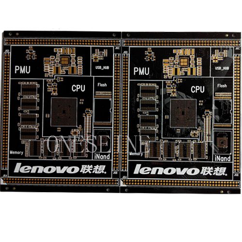
Description
*6 Layer Via In Pad PCB Multilayer Computer Printed Circuit
Board Manufacture
PCB board description:
Layer:*6
Material:FR4 Isola
Surface finish: immersion gold
Solder mask:Black
Min line:3mil
Min hole:0.*5mm
Copper weight:1OZ
Board size:*0**5CM
Via in pad PCB:
via-padsIn PCB design, via refers to a pad with a plated hole that
connects copper tracks from one layer of the board to other
layer(s). High-density multi-layer PCBs may have blind vias, which
are visible only on one surface, or buried vias, which are visible
on neither, normally referred to as micro vias. The advent and
extensive use of finer pitch devices and requirements for smaller
size PCBs creates new challenges. An exciting solution to these
challenges uses a recent, but common PCB manufacturing technology
with self descriptive name, via in pad.
Via in pad helps to reduce inductance, increase density and employ
finer pitch array packages. The via in pad approach places a via
directly under the devices contact pads. This allows higher
component density and improved routing. Consequently, via in pad
provides the designer significant PCB space savings. For example,
traditional fan-out places four components, whereas with via in
pad, six components can be placed within the same board
outline.
Filled via in pad is a way to achieve intermediate density with an
intermediate cost compared to using blind/buried vias. Some of the
key advantages associated with using the via in pad technology
are:
Fan out fine pitch (less than .*5mm) BGAs
Meets closely packed placement requirements
Better thermal management
Overcomes high speed design issues and constraints i.e. low
inductance
No via plugging is required at component locations
Provides a flat, coplanar surface for component attachment
The benefits of via-in-pad designs are well documented. From
reduction of inductance to increased density, via-in-pad has become
an essential tool for designers when navigating the routing
challenges of fine pitch array packages that have become mainstays
in todays BOMs but there are trade-offs that must be
considered.
The basic concept is elegant. The via-in-pad design methodology
allows the designer to place the via right beneath the component
contact pad. Hence the reduction of inductance plus the added
benefit of improved routing density which can lead to higher
density per layer. The net result is more routing in less space and
a smaller PCBs footprint. It is another miniaturization tool that
can drive cost down.
However, there are trade-offs when implementing via-in-pad
technology. The process may increase the PCB cost. The reason is
that the via-in-pad technique requires both additional process
steps and extra materials. Added costs are found in both the extra
materials used, including epoxy or metal based via fill materials
and copper cap plating processes, as well as added process steps
like vacuum via fill, curing, planarization and secondary plating
operations. There is also the general challenge that results from
producing a higher density PCB.
Computer PCB boards:
Prior to the invention of the microprocessor PCB, a computer
consisted of multiple printed circuit boards in a card-cage case
with components connected by a backplane, a set of interconnected
sockets. In very old designs the wires were discrete connections
between card connector pins, but printed circuit boards soon became
the standard practice PCB. The Central Processing Unit, memory and
peripherals were housed on individual printed circuit boards which
were plugged into the backplate.
During the late ***0s and ***0s, it became economical to move an
increasing number of peripheral functions onto the motherboard. In
the late ***0s, personal computer motherboards began to include
single ICs (also called Super I/O chips) PCB capable of supporting
a set of low-speed peripherals: keyboard, mouse, floppy disk drive
PCB, serial ports, and parallel ports. By the late****0s, many
personal PCB computer motherboards supported a full range of audio,
video, storage, and networking functions without the need for any
expansion cards at all; higher-end systems for 3D gaming and
computer graphics typically retained only the graphics card as a
separate component PCB.
The most PCB popular computers such as the Apple II and IBM PC had
published schematic diagrams and other documentation which
permitted rapid PCB reverse-engineering and third-party replacement
motherboards. Usually intended for building new computers
compatible with the exemplars PCB, many motherboards offered
additional performance or other features and were used to upgrade
the manufacturer\'s original equipment.
skype:oneseine-sales