La description
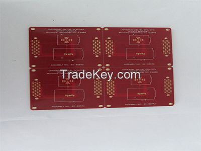
HDI PCB
Specification
High density interconnect (HDI) PCBs represent one of the
fastest-growing segments of PCB market. And its design is
able to incorporate finer lines and spaces, smaller vias and
capture pads, and higher connection pad densities because of
the higher circuitry density. A high density PCB features blind and
buried vias and often contains micro vias that the diameter is
.**6 or even less.
Key HDI PCB
Benefits
The evolution of high density PCB technology has given engineers
more imagination and flexibility than ever before. Designers
now have the ability to put more components on both sides of the
raw PCB if needed. In essence, an HDI PCB gives designers more
space to work with and allows them to put smaller
components much closer together. This final results in faster
signal transmission will go along well with enhanced signal
quality.
HDI PCB is widely used to reduce the weight and overall dimensions
of products as well as enhancing the electrical performance of the
device. It's regularly found in mobile phones, touch-screen
devices, laptop computers, digital cameras, 4G network
communications, and prominently featured in medical devices,
various electronic aircraft parts and components.
High Density PCB of
Impeccable Quality
Over the course of a decade in business, Flying has established a
hard-earned reputation for manufacturing PCB with the
highest quality. Our customized PCB manufacturing capabilities
enable you to get the finest quality at competitive prices without
min quantity requirements. Our team will run for your PCB files,
check your design work and consult with you to ensure that it is
ready for manufacturing, and that your boards will meet your
performance requirements. We also have an on-site quality control
department to verify your finished products and meet your high
quality standards.
| Item |
Capability |
| Number of Layers |
***4layers |
| Order Quantity |
1pc*****0+pcs |
| Material |
FR*4 standard Tg**0ºC,FR*4 High Tg**0ºC,FR*4 and Rogers
combined lamination |
| Board Thickness |
0.*2''*0.*2''(0.4mm*3.0mm) |
| Copper Weight |
0.5oz*2.0oz(*8μm**0μm) |
| Min Drilling Hole Diameter |
6mil(0.*5mm),4mil(0.*0mm)-laser drill |
| Surface Finish |
HASL-Hot Air Solder Leveling
Lead Free HASL-RoHS
ENIG-Electroless Nickle/Immersion Gold-RoHS
Immersion Silver-RoHS
Immersion Tin-RoHS
OSP-Organic Solderability Preservatives-RoHS |
| Pays: |
China |
| N ° de modèle: |
-
|
| Prix FOB: |
(Negotiable)
Obtenir le dernier prix
|
| Localité: |
- |
| Prix de commande minimale: |
- |
| Commande minimale: |
- |
| Packaging Detail: |
- |
| Heure de livraison: |
3 to 5 days |
| Capacité de Fournir: |
- |
| Payment Type: |
- |
| Groupe de produits : |
- |


 2 layers-10 layers")
