Prix FOB
Obtenir le dernier prix1 ~ 560 / Piece
|1 Square Meter Minimum Order
Pays:
China
N ° de modèle:
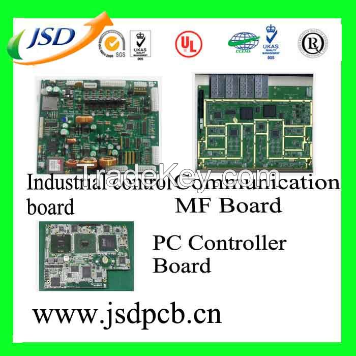
PCB JSD
Prix FOB:
1 ~ 560 / Piece Obtenir le dernier prix
Localité:
Shenzhen, China
Prix de commande minimale:
1 per Piece
Commande minimale:
1 Square Meter
Packaging Detail:
Vacuum packing, Plastic bag inside, standard carton packing outside
Heure de livraison:
2~8days for common, other customized
Capacité de Fournir:
5000 Square Meter per Month
Payment Type:
T/T, L/C, Western Union, PayPal
Groupe de produits :
Personne à contacter Jessica
Shenzhen, Guangdong
| Pays: | China |
| N ° de modèle: | PCB JSD |
| Prix FOB: | 1 ~ 560 / Piece Obtenir le dernier prix |
| Localité: | Shenzhen, China |
| Prix de commande minimale: | 1 per Piece |
| Commande minimale: | 1 Square Meter |
| Packaging Detail: | Vacuum packing, Plastic bag inside, standard carton packing outside |
| Heure de livraison: | 2~8days for common, other customized |
| Capacité de Fournir: | 5000 Square Meter per Month |
| Payment Type: | T/T, L/C, Western Union, PayPal |
| Groupe de produits : | PCB |


 2 layers-10 layers")
